
Changing the rules for LEDs
GaN and Silicon really shouldn’t go together but several companies are making it work in order to reap the cost benefits, as Sally Ward-Foxton reports.
With packaged LEDs set to reach a market size of $16bn (USD) by 2018 (up from $13.9bn (USD) in 2013), the demand for LED lighting is growing fast. Technology advances are making LEDs brighter and longer-life, making them suitable for many more applications. Now it seems that technology has also found a way to make these already mass-produced components even cheaper.
In the current process, the Gallium Nitride (GaN) required for high-brightness white LEDs is grown on either sapphire or silicon carbide (SiC) substrates. Wafers made of these materials are relatively expensive and until recently were only available in smaller sizes (4"). It would be much cheaper if GaN could be grown successfully on ordinary silicon (Si) wafers, which are easy to make in larger sizes.
“The main cost factors are the material cost of wafers and the wafer size; in our case this is 8", which results in a higher number of chips per wafer,” says Matthias Diephaus, Senior Manager of Opto Semiconductors at Toshiba Electronics Europe.
Larger wafers are more economical, since it takes almost as long to process a 6" wafer as a 4" one, but the surface area is four times as large, almost quadrupling throughput. Silicon wafers are available cheaply in high volumes and existing, fully depreciated silicon CMOS fabs could be used to make LEDs, bringing down price.
The trouble is, growing GaN on silicon wafers is not easy. The crystal lattice structures don’t match, and the mismatch causes tensile strain. The thermal coefficients of the materials are also very different. The wafers bend, and cracks form, lowering the yield substantially.
To bridge the gap between the two lattices, a buffer layer can be used. The exact materials used in these proprietary buffer layers are top secret, but it’s a reasonable assumption that the lattice spacing in the buffer layer is between that of the Si and that of the GaN, to reduce the tensile strain between each of the layers. Other techniques involve placing the Si wafer under strain to cancel out the tensile strain when the materials cool.
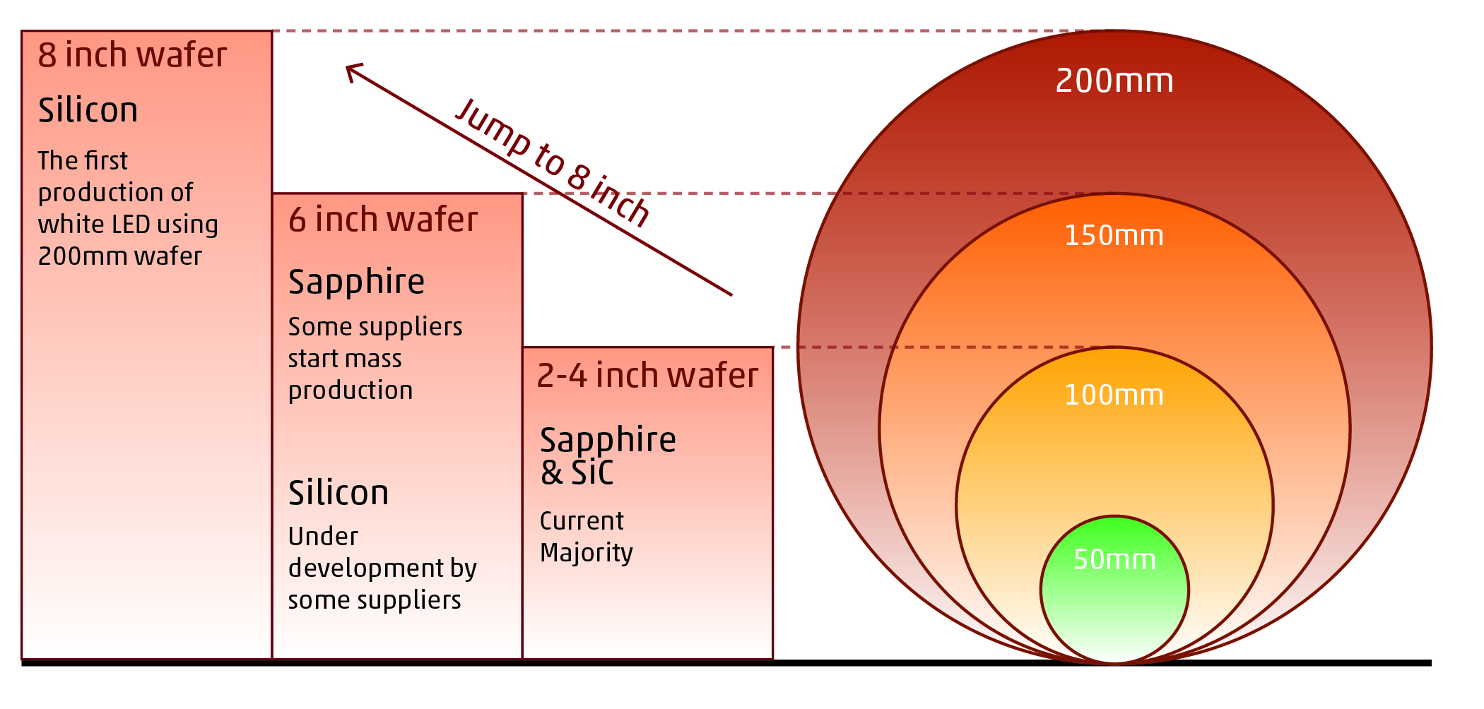 Figure 1: Today’s situation is that some suppliers are starting mass production on 6" sapphire wafers. Meanwhile, Toshiba was the first to produce GaN LEDs on 8" silicon wafers
Another problem with silicon is that it readily absorbs photons, so it would absorb all the light produced by the GaN device, crippling the overall efficacy. For this reason, a mirror layer is required to make sure all the light is reflected back out of the device.
Even with the additional process steps relating to the buffer layer and the mirror layer, supporters of the technology say there is a large economic advantage to using GaN-on-Si technology.
Improving efficacy
The first company to produce GaN LEDs on 8" silicon wafers was Toshiba (Figure 1).
Toshiba’s process is based on the work of Bridgelux; the two companies have been working together since the start of 2012, and Toshiba acquired Bridgelux in May 2013. The latest devices to come out of this process are actually the second generation of Toshiba’s LETERAS series, the TL1F2 series (Figure 2). These 1W LEDs cost just €0.20 in volume, according to Diephaus.
Compared to the first generation of this technology, Toshiba has improved luminous efficacy to as much as 135lm/W, depending on the colour temperature and colour rendering index required. This has been achieved by optimising the packaging and increasing the optical power of the GaN-on-Si LED chips. They are aimed at lamps, ceiling lighting, street lights and floodlights.
An alternative process conceived by British startup CamGaN is being developed by Plessey Semiconductors after it acquired CamGaN in 2012.
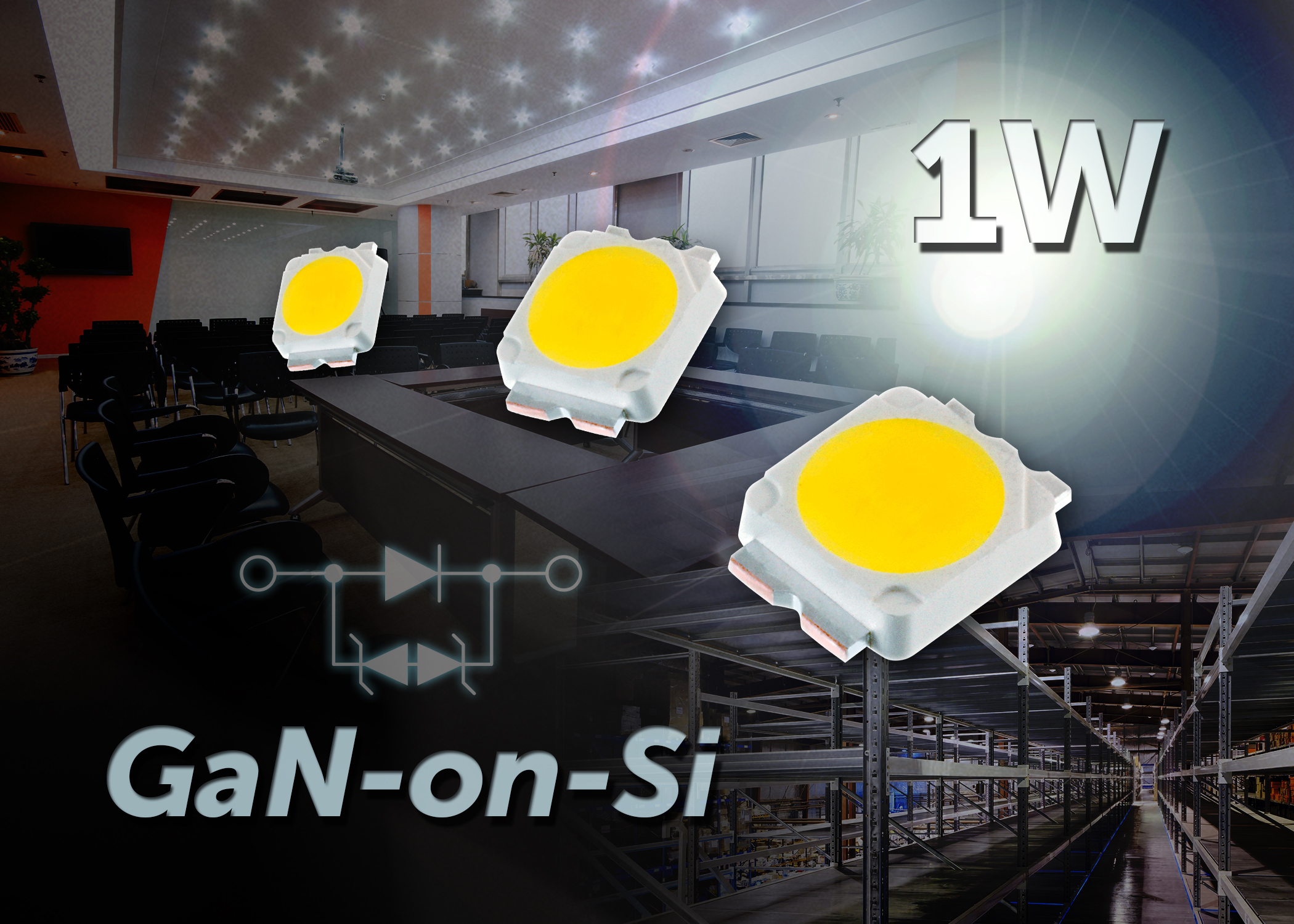
Figure 2: Toshiba’s LETERAS devices are suitable for lamps, ceiling lighting, street lights and floodlights
“Plessey uses a buffer-layer and other proprietary techniques to ensure that we achieve high quality GaN and minimal wafer bowing — less than 20µm over a 6" wafer,” explains Dr Keith Strickland, CTO of Plessey Semiconductors.
Plessey’s process uses a thinner GaN layer than most — around 2.5µm for the buffer layer and epilayer compared to 8µm for other processes. This helps reduce costs further.
“The thinner the GaN layer the quicker the wafer can be grown, which leads to a shorter cycle-time,” Dr Strickland explains. “This in turn leads to an increase in the number of wafers per week from our reactor and hence a lower cost per LED. The techniques by which we can achieve a thinner GaN layer are specifically developed by Plessey.”
Current Plessey devices perform in the range of 60-80lm/W and are built on the company’s 6in wafer line in Plymouth. As an example, the PLW114050 white LED from the company’s MAGIC series is available now and costs £0.10 (about €0.12) in quantities of 1000 or more. The company’s roadmap includes a path to 8" wafers; luminous efficacy is set to reach 100-120lm/W by mid 2014, and 150lm/W by end of 2014 (Figure 3).
“There are many factors that influence performance, but once a solution to the growth of good quality GaN onto a silicon substrate is achieved, the basic GaN LED stack is reasonably standard across different platforms,” Dr Strickland adds. “Plessey is progressing rapidly in the development of its LED stack to levels comparable to the leading Sapphire technologies available today.”
Economic benefits
However, there has been some discussion about whether GaN-on-Si is a cheaper long-term option. Critics argue that wafer cost is only a small proportion of the overall cost of the finished luminaire assembly, and that sapphire and SiC have established processes which are already producing high yields. By comparison, GaN-on-Si is a relative newcomer.
The other problem for GaN-on-Si is that sapphire wafers are getting bigger and cheaper all the time, with 6" sapphire wafers readily available today. Will this result in a reduced opportunity for GaN-on-Si?
“It is still difficult to judge,” said Toshiba’s Matthias Diephaus. “Of course, there is a great deal of price pressure in the market and our competitors are making efforts to reduce costs. Moving to 6in sapphire wafers seems to be one of the measures being adopted. There will be more chips per wafer but the cost for a 6" sapphire wafer might still be rather expensive as it is not yet used in large volumes.”
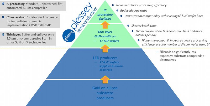
Figure 3: Plessey’s GaN-on-Si offering uses a thinner GaN layer to increase productivity
“Silicon wafers have a cost level significantly lower than sapphire and are easier to manufacture in automated production lines,” Plessey’s Dr Strickland adds. “8" silicon wafers are readily available today and Plessey also has an 8" line that we can bring online once we have reached full volume production on our current 6" line.”
Sapphire and SiC still represent the bulk of sales of White LEDs today. The ultimate success of GaN-on-Si depends on matching the performance of LEDs from the more established processes while maintaining its economic advantages, but whether that can be realised remains to be seen.
GaN-on-GaN
Why use a substrate at all when you can use bulk GaN to make LEDs? The answer is, because it’s rather expensive. However, there are upsides to the technology. The GaN bulk substrate has none of the problems associated with GaN-on-substrate such as cracking or bending wafers. Devices are developed with hardly any defects and can therefore be driven at higher current densities to make them run brighter - fewer individual LEDs are needed for the same light output, potentially saving money. For example, California-based Soraa has developed LEDs that run ten times brighter than conventional LEDs using this technique. However, this technology has thus far been seen as rather niche, and will likely be restricted to very high-end applications for the time being.
Product Spotlight
APV1111GVY
Panasonic

Panasonic PhotoMOS® Photovoltaic MOSFET High-Power Drivers
| SKU: | |
|---|---|
| Stock: | 3490 |
| Cost: | $3.95 |
